
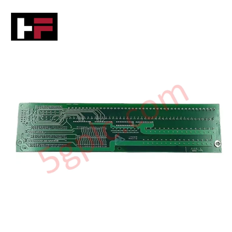
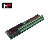
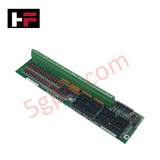
Product Details
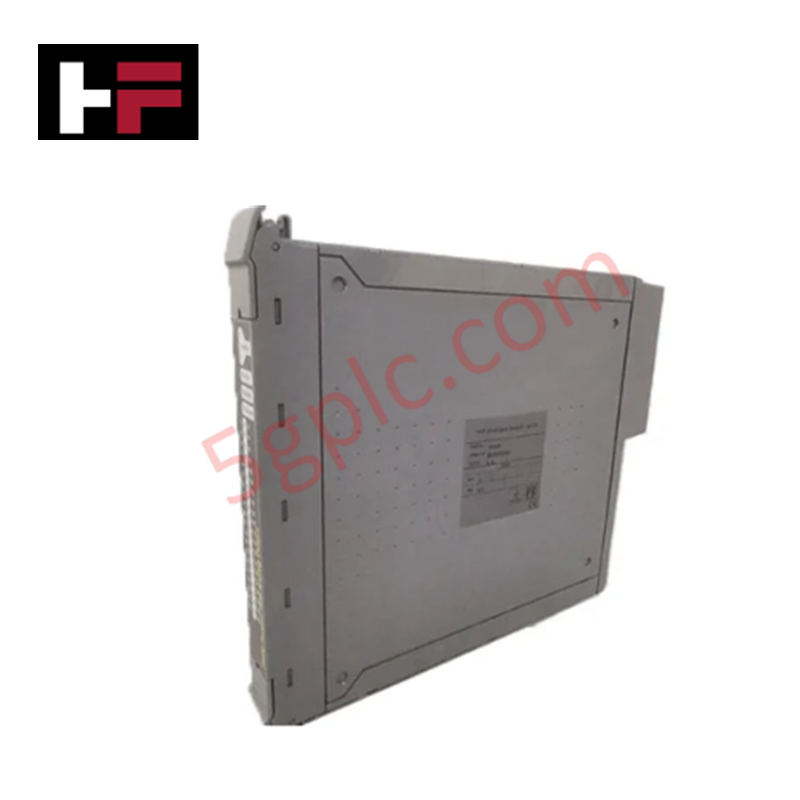
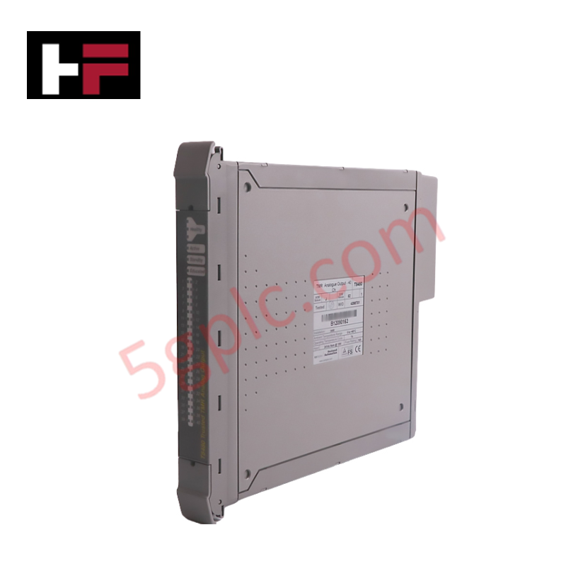
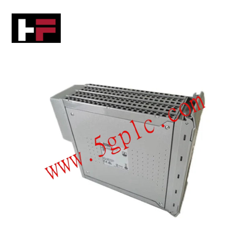
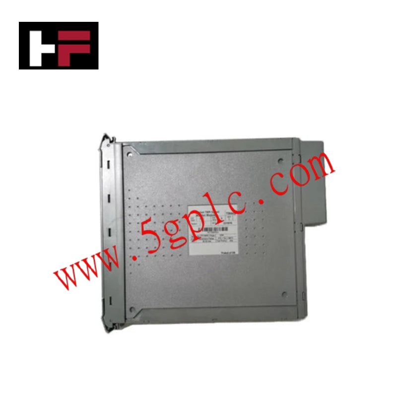
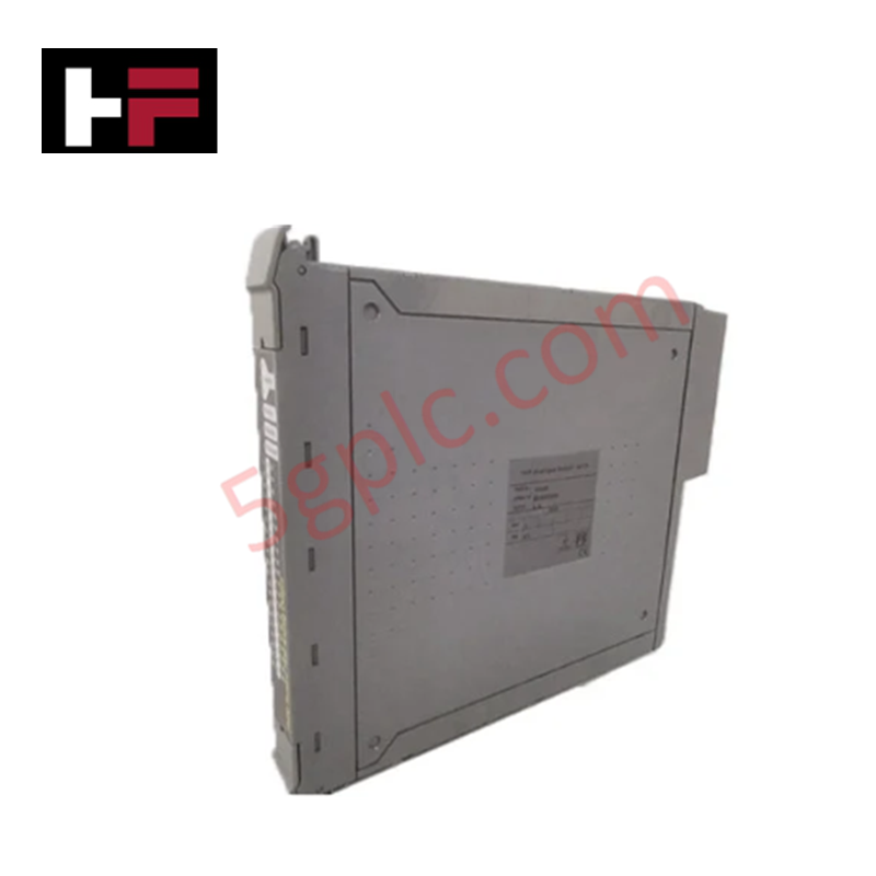
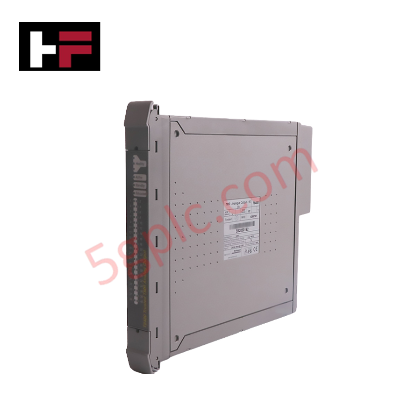
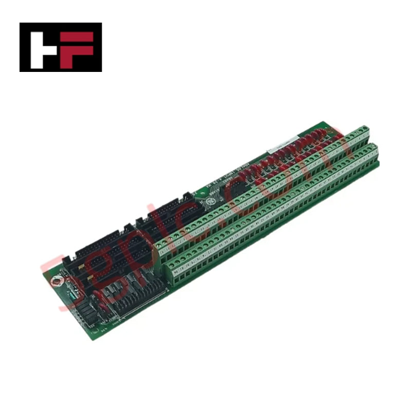
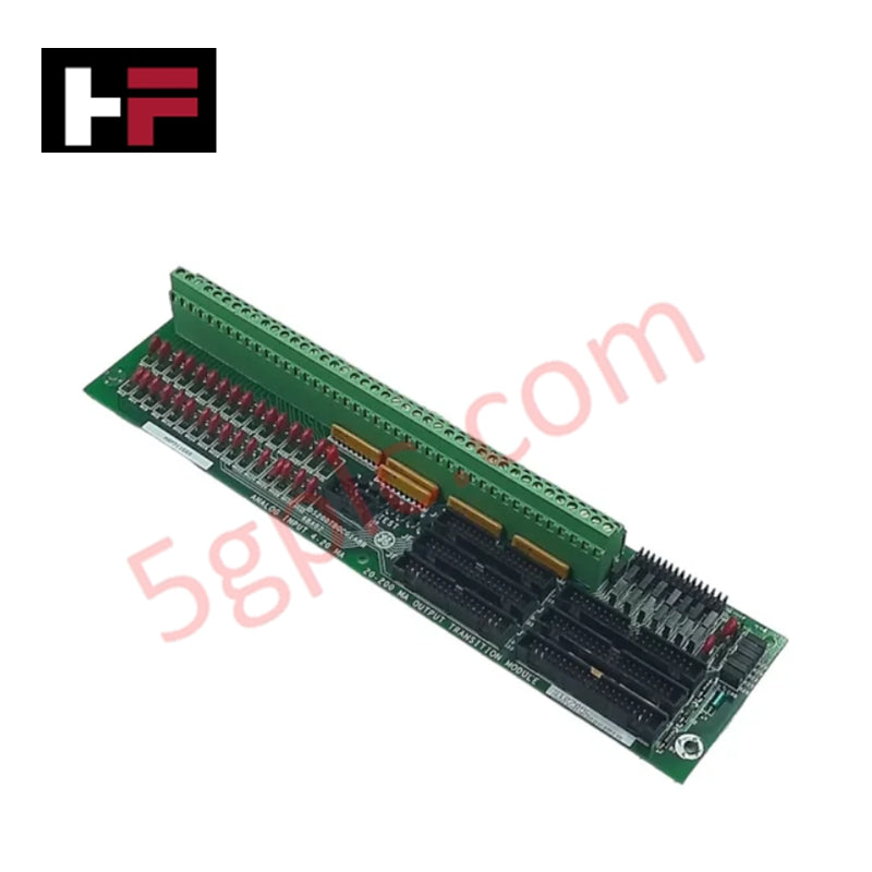
Configured for signal termination and scaling in Mark V control systems, the GE DS200TBQCG1A (DS200TBQC Analog Input/Output Termination Module) provides direct physical execution of LVDT/R and 4-20 mA signal routing between field devices and the TCQA processing core.
Hardware Specifications
| Parameter | Specification |
|---|---|
| Model | DS200TBQCG1A |
| Brand | General Electric |
| Origin | USA |
| Operating Temp | Standard industrial range |
| Power Consumption | Not specified |
| Terminal Blocks | 2 blocks (TB1, TB2), 83 terminals each (166 total) |
| Connectors | 3 x 40-pin, 3 x 34-pin |
Industrial Control and Firmware Flash Compatibility
The DS200TBQCG1A manages critical analog data exchange between the TCQA boards located in the R1, R2, and R3 cores. Deterministic signal handling is supported by hardware-defined pathways: the JBR connector facilitates bi-directional 4-20 mA loop communication, while the JFR connector handles LVDT/R position input processing. The board architecture allows for I/O density scaling through 166 discrete terminal points. Firmware flash compatibility is not applicable, as signal conditioning logic is executed via physical hardware jumpers that determine output current ranges (20 mA or 200 mA maximum). This hardwired configuration ensures that scaling parameters remain fixed regardless of processor state, providing consistent feedback to the control core.
Frequently Asked Questions
Q: Can the output current range be modified through system software?
A: No. Output current range selection (20 mA or 200 mA maximum) is managed exclusively by physical hardware jumpers on the TBQC board. These must be verified against the specific field device requirements prior to commissioning.
Q: What is the purpose of the 15 onboard jumpers?
A: The 15 jumpers are provided for the manual configuration of circuit paths and signal scaling options. Most settings are factory-configured for specific core-to-TCQA signal requirements and should not be modified without explicit reference to the control system schematic.
Field Installation Guidelines
- De-energize the Mark V R1, R2, and R3 cores entirely before accessing the TBQC board to prevent damage to the TCQA interface or shorting of the 4-20 mA analog loops.
- Verify all field wiring at the TB1 and TB2 terminal blocks; ensure that high-level analog signals are shielded and that the shields are bonded to the designated chassis ground to prevent electromagnetic interference.
- Handle the module by the edges and use electrostatic discharge (ESD) mitigation techniques to protect the high-density connector interfaces.
- Ensure all ribbon cables (connected to JBR, JFR) are fully seated and locked into their headers to guarantee reliable signal transmission between the termination module and the processing core.
Additional Information
- 100% Genuine Parts: All products are original and authentic, ensuring reliable industrial performance.
- 30-Day Refund Guarantee: Return any in-stock item within 30 days in original, unopened packaging for a full refund (excluding shipping and fees).
- 12-Month Warranty: Covers defects in materials or workmanship; excludes misuse, normal wear, or unauthorized modifications.
- Worldwide Shipping: We ship via USPS, UPS, FedEx, and DHL. Delivery times vary by country and may be subject to customs or import fees.
- Support & Contact: Technical and warranty assistance is available anytime. Contact us here: Contact.
- Purchase Guidance: Check product specifications and compatibility carefully before ordering to ensure proper application.


Tech & Buying Guide

Understanding Marshalling Cabinets in Industrial Automation and Control Systems
Marshalling cabinets serve as the crucial connection hub between field instruments and centralized processing units. In large DCS and PLC control system architectures, hundreds of multipair field cables run from local junction boxes to the central instrument equipment room. The marshalling cabinet houses field terminal blocks, surge arresters, intrinsic safety isolation barriers, and interposing relays. By segregating field field-wiring terminations from sensitive processor hardware, engineers protect expensive controller backplanes from high-voltage transients. Consequently, this modular separation dramatically streamlines maintenance workflows and simplifies system expansion.

Essential Best Practices for PLC Wiring and Installation in Industrial Automation
Successful control system deployment begins with thoroughly reviewing manufacturer technical documentation. Controllers from major brands like Allen-Bradley, Siemens, and Schneider Electric feature unique terminal layouts. Engineers must verify voltage requirements before connecting power cables to prevent catastrophic equipment damage. Standard line connections require strict adherence to regional electrical codes and proper wire color coding. Furthermore, panel builders should always establish a robust low-impedance ground connection using at least 16-AWG copper conductor tied directly to the main plant grounding grid.

Demystifying Programmable Logic Controllers: Comprehensive Guide to PLC Classification and Selection in Industrial Automation
Modern industrial automation heavily relies on Programmable Logic Controllers (PLCs) to drive factory floor efficiency. Over my 15 years as an industrial automation expert working with DCS, TSI, and control systems, I have seen PLCs evolve into the central nervous system of modern manufacturing. Selecting the right controller requires a deep understanding of PLC types based on physical size, hardware architecture, and power supply configurations.