
Product Details
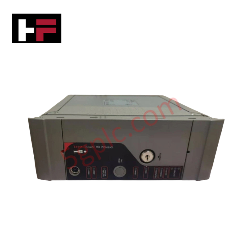
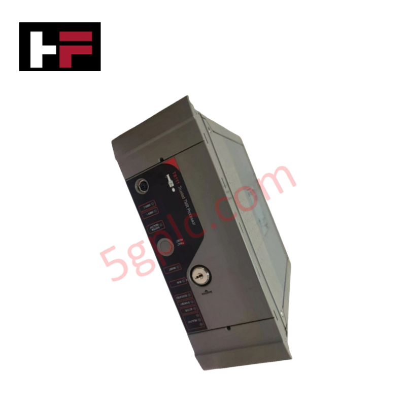
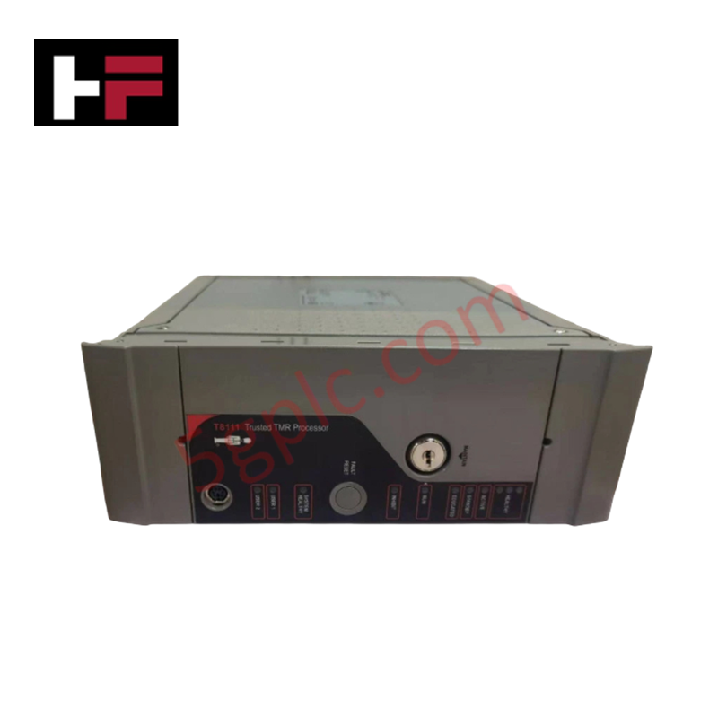
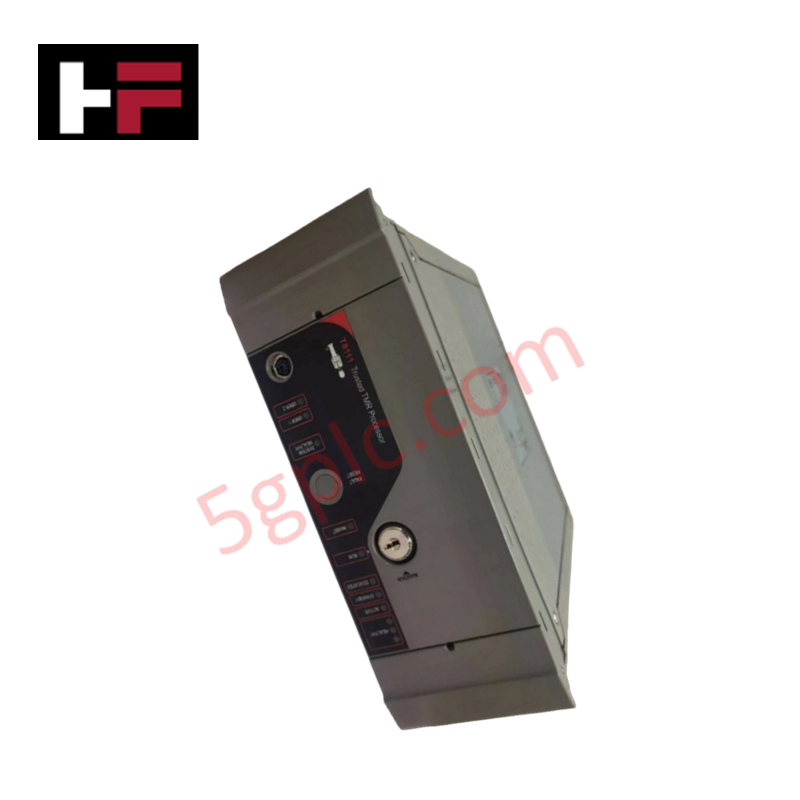
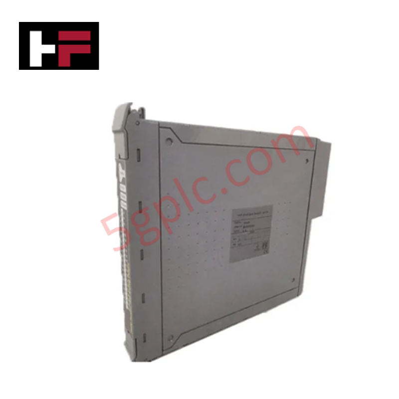
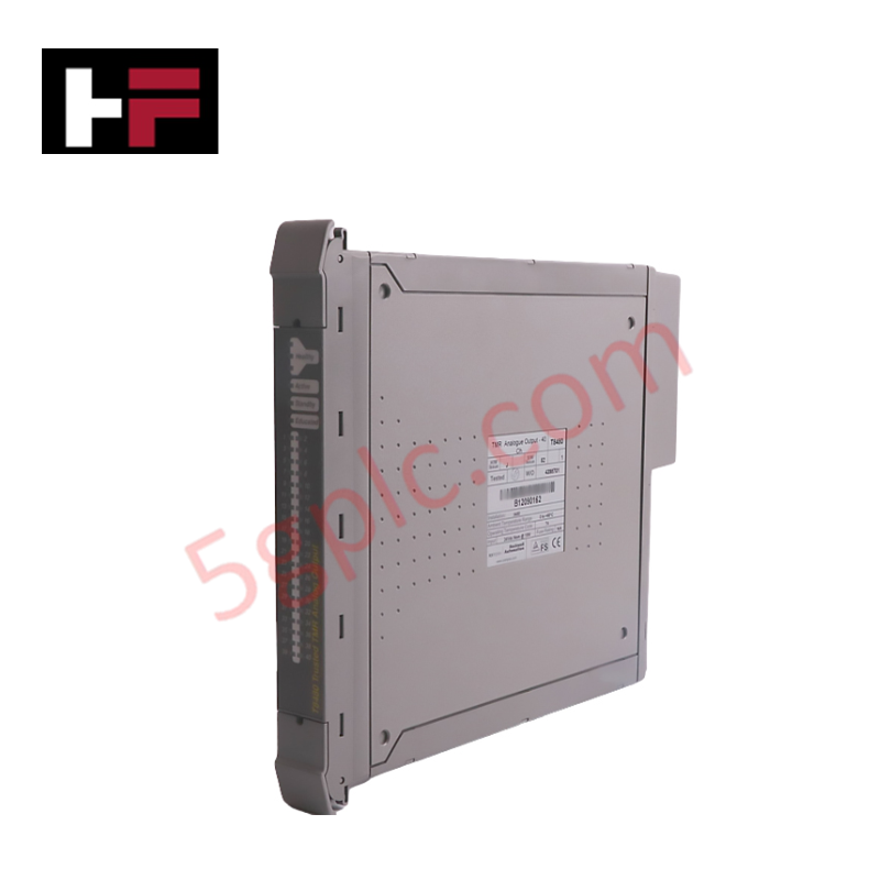
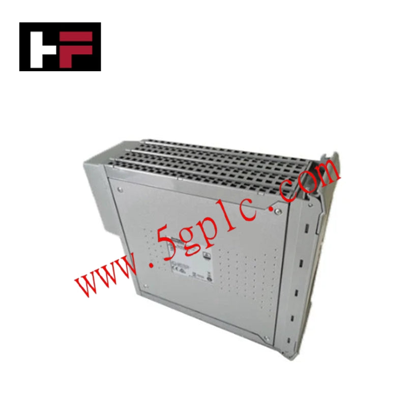
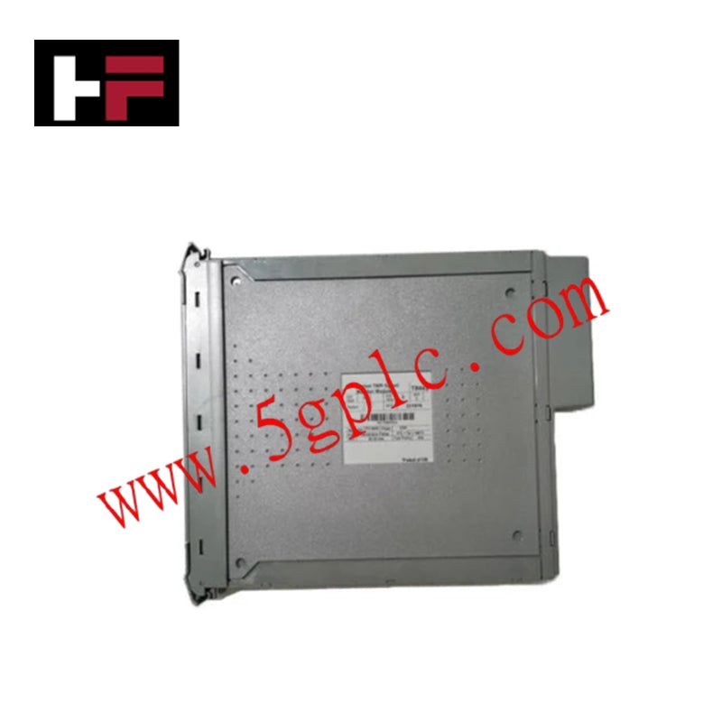
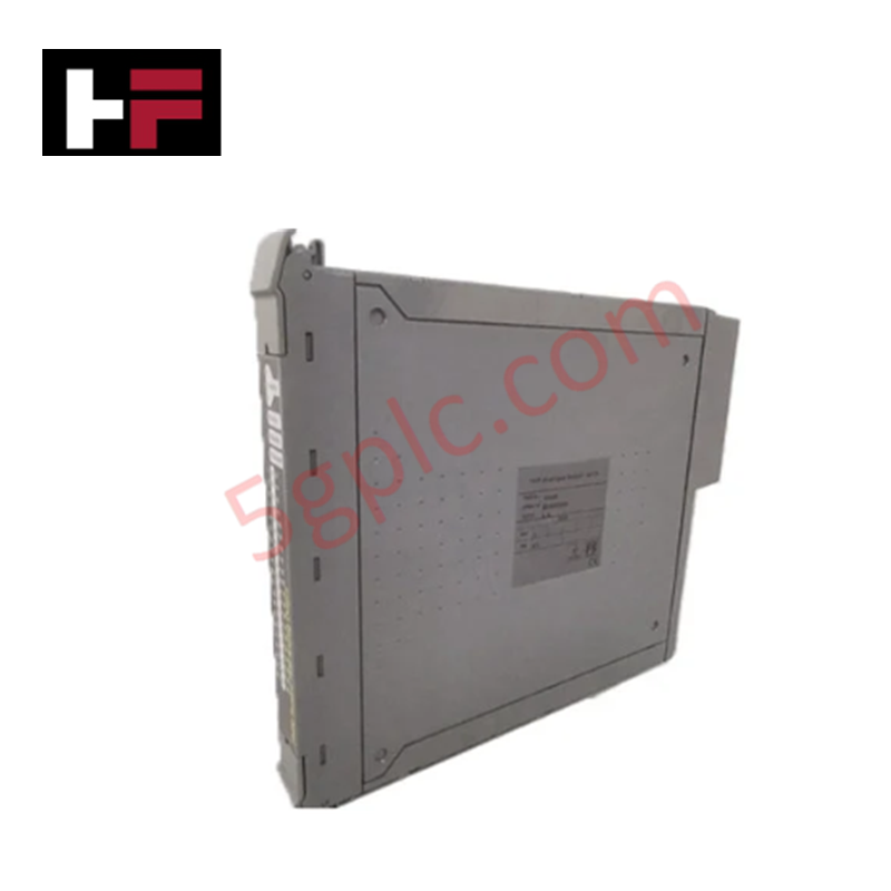
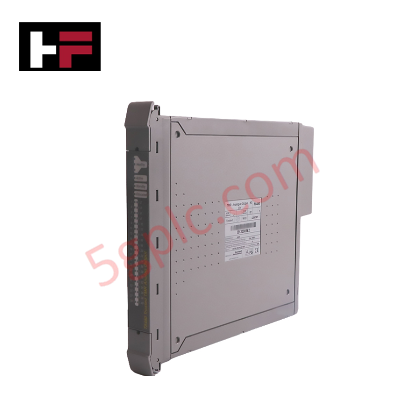
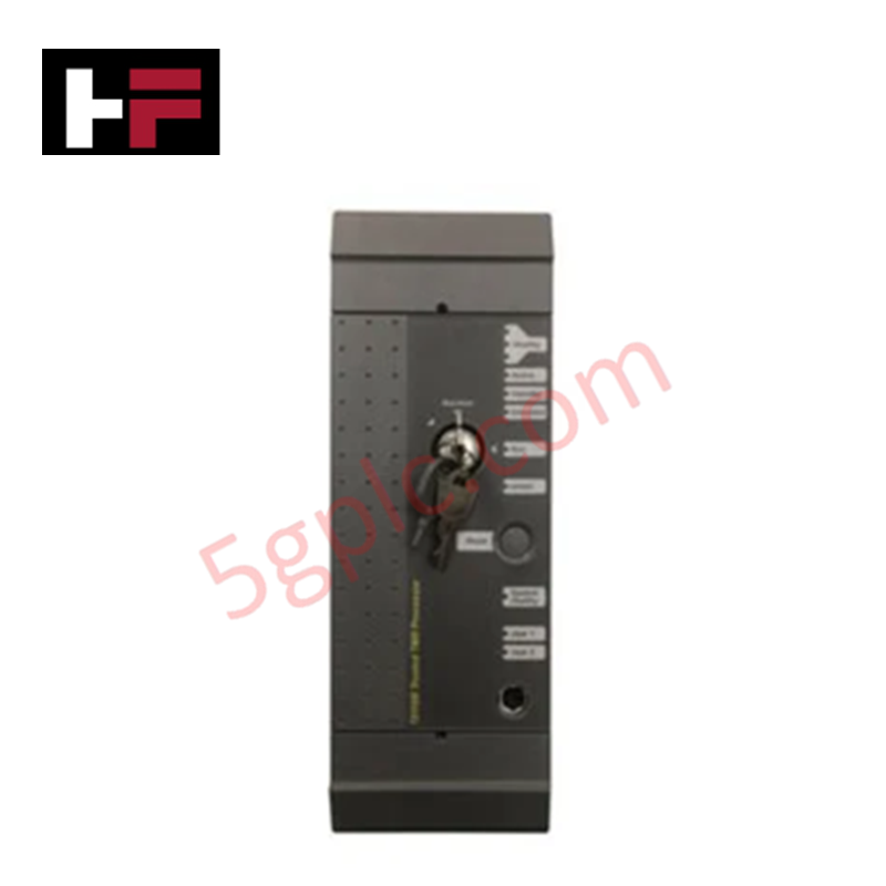
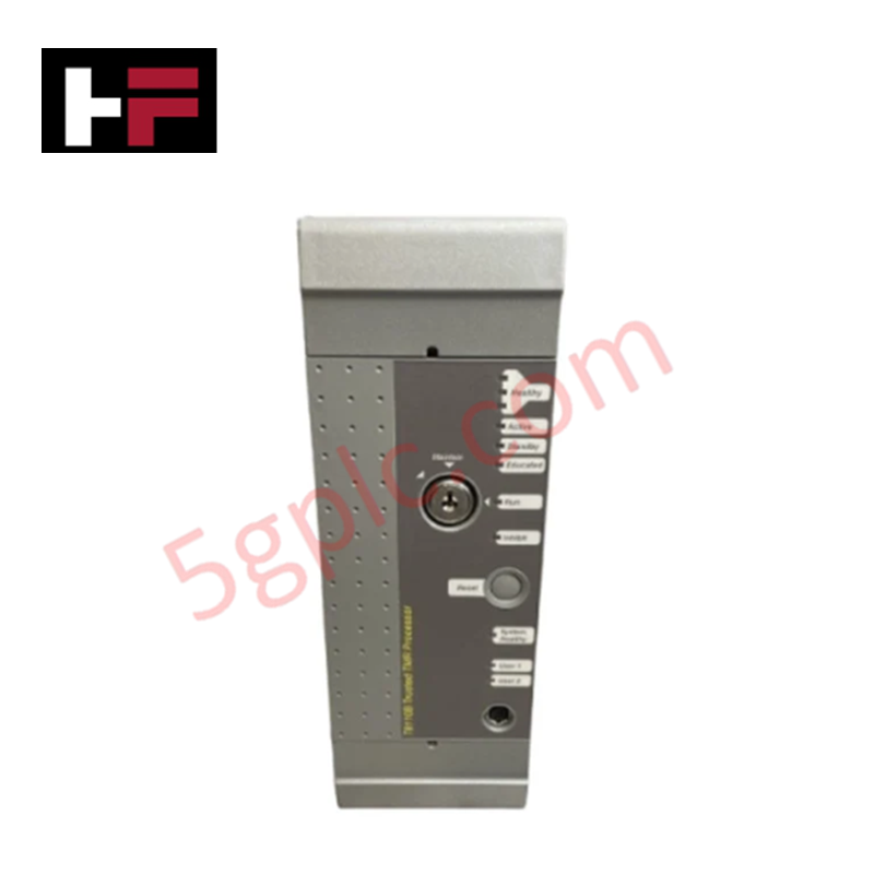
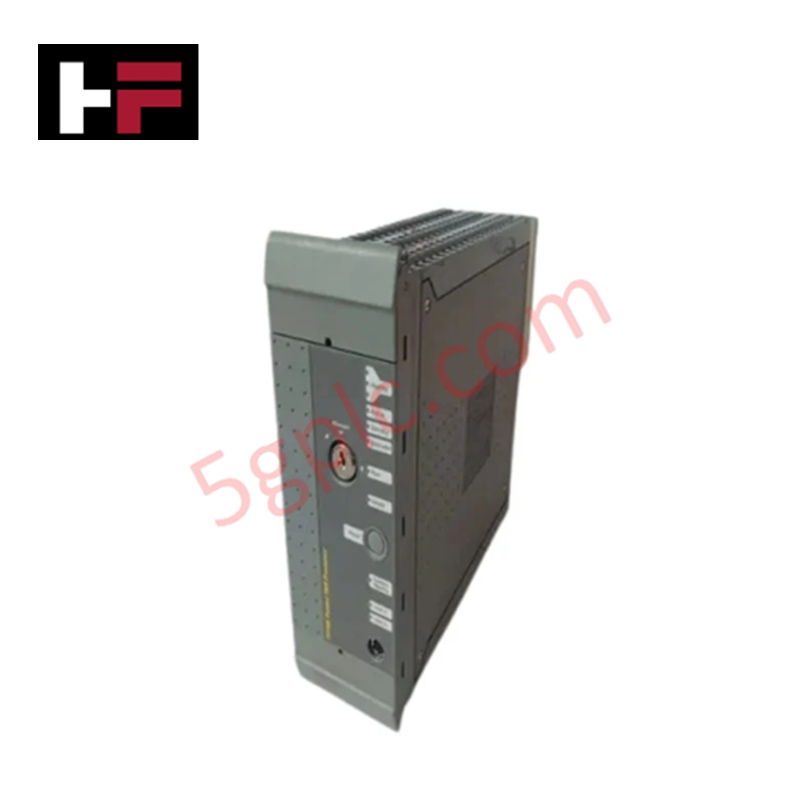
The ICS Triplex T8110B, also cataloged as the T8110B Trusted TMR Processor Module, operates as a dedicated hardware component for safety logic execution within T8100 chassis platforms. Executing logic across a triple redundant Inter-Module Bus, the unit processes application code via a 100 MHz clock rate paired with 16 MB EDO DRAM and 128 kB NVRAM variable memory.
Hardware Specifications
| Parameter | Specification |
|---|---|
| Model | T8110B |
| Brand | ICS Triplex |
| Origin | United Kingdom |
| Weight | 2.94 kg (6.48 lb) |
| Dimensions | 266 mm x 93 mm x 303 mm (10.5 in x 3.6 in x 12.0 in) |
| Operating Temp | 0 deg C to +60 deg C (+32 deg F to +140 deg F) |
| Power Consumption | 80 W Maximum Load (Heat Dissipation: 80 W) |
| Voltage Range | 20 VDC to 32 VDC |
| Compatible Chassis | T8100 |
| Processor Clock | 100 MHz |
| Memory Configuration | 16 MB EDO DRAM (60 ns), 2 MB FLASH, 512 kB EPROM, 128 kB NVRAM |
| SOE Buffer Capacity | 1000 events (transfers to CI buffer of 4000 events) |
| Retained Variable Storage | Booleans: 1 byte, Analogues: 4 bytes, Timers: 5 bytes |
| I/O Interface | Triple redundant Inter-Module Bus |
| Relative Humidity | 10% to 95% non-condensing |
High-Reliability Safety Control & TMR Architecture
The T8110B implements a triple modular redundancy (TMR) 2oo3 architecture to satisfy SIL3 certification criteria across high-availability safety applications. Fault-tolerant processing circuits execute synchronized 2oo3 voting across internal bus lanes, guaranteeing fail-safe state execution without interruption to active control loops. Galvanic isolation throughout system interfaces prevents localized electrical transients from crossing bus boundaries, maintaining determinism during high-density I/O scan cycles.
Frequently Asked Questions
Q: How are retained variables allocated within the T8110B non-volatile memory structure?
A: Retained variable memory uses specific footprint allocations: 1 byte per Boolean variable, 4 bytes per Analogue variable, and 5 bytes per Timer variable within the 128 kB NVRAM space.
Q: What is the sequence of events (SOE) storage architecture on the processor module?
A: The T8110B maintains an onboard SOE buffer capacity of 1000 events, which automatically transfers logged event records to a Communications Interface (CI) buffer capable of storing up to 4000 events.
Q: Can the T8110B processor module be deployed in secondary expansion chassis?
A: No. The T8110B processor module is designed specifically for operation inside the primary T8100 system chassis.
Field Installation Guidelines
- Ensure the T8100 chassis backplane power is verified within the 20 VDC to 32 VDC supply tolerance before inserting the module.
- Torque the top and bottom chassis module retention screws to ensure positive frame ground contact and mechanical latching to the backplane connectors.
- Maintain unrestricted vertical airflow above and below the T8100 chassis slot to dissipate up to 80 W of thermal load during full logic processing.
- Verify system earthing connections to mitigate high-frequency ground noise that could affect time synchronization across the triple redundant bus.
Additional Information
- 100% Genuine Parts: All products are original and authentic, ensuring reliable industrial performance.
- 30-Day Refund Guarantee: Return any in-stock item within 30 days in original, unopened packaging for a full refund (excluding shipping and fees).
- 12-Month Warranty: Covers defects in materials or workmanship; excludes misuse, normal wear, or unauthorized modifications.
- Worldwide Shipping: We ship via USPS, UPS, FedEx, and DHL. Delivery times vary by country and may be subject to customs or import fees.
- Support & Contact: Technical and warranty assistance is available anytime. Contact us here: Contact.
- Purchase Guidance: Check product specifications and compatibility carefully before ordering to ensure proper application.


Tech & Buying Guide

Hub vs Switch vs Router in Industrial Automation Architecture
Modern factory automation relies on reliable industrial networking infrastructure to exchange real-time field data across operational technology systems. Engineers often encounter networking hardware like hubs, switches, and routers when integrating Programmable Logic Controllers, Distributed Control Systems, and SCADA monitoring nodes. Although these devices share physical ports, they operate at different layers of the Open Systems Interconnection reference model and deliver distinct traffic management capabilities.

Marshalling Cabinet Preventive Maintenance: Essential Healthiness Checks for PLC, DCS, and ESD Systems
Marshalling cabinets serve as the vital interface between field instrumentation and control room electronics in modern process facilities. Regular preventive maintenance of these cabinets ensures signal integrity across programmable logic controllers (PLCs), distributed control systems (DCS), and emergency shutdown (ESD) networks. System technicians must execute structured inspection protocols to mitigate environmental risks, identify loose wiring, and maintain continuous operational readiness.

Spatial Computing in Industrial Automation: Elevating PLC and DCS Operations with AR and VR
Industry 4.0 integrates digital intelligence into field operations, transforming factory automation landscapes worldwide. Spatial technologies—specifically Augmented Reality (AR) and Virtual Reality (VR)—redefine how engineers interact with industrial control systems. By bridging computer-generated CAD models with real-time operational technology (OT) data, immersive displays enable intuitive monitoring, rapid diagnostics, and safer maintenance across complex processing facilities.